▪ Two supply voltage options:
• 2.7 V – 3.6 V
• 2.5 V – 3.6 V
▪ Serial Peripheral Interface (SPI) Compatible
• Supports SPI modes 0 and 3
• Supports dual output operations (1,1,2)
• Supports quad output operations (1-1-4)
• Supports quad I/O / XiP operations (1-4-4, 0-4-4)
▪ 108 MHz maximum operating frequency
▪ Read operations
• Fast read up to 108 MHz
• Continuous read (with 8/16/32/64-byte wrap)
▪ Flexible erase architecture and time
• Sector erase 4 kB: 50 ms (typical)
• Block erase 32 kB and 64 kB: 120 ms and
200 ms (typical)
• Full chip erase: 5.5 seconds (typical)
▪ Flexible programming and time
• Page/byte program: from 1 to 256 bytes
• Page program time: 0.4 ms (typical)
▪ Erase program suspend resume
▪ JEDEC Standard Manufacturer and Device ID
▪ Memory protection support
• User-definable protected area at start or end of
memory array
• Enable/disable protection with WP pin
▪ 3 x 256-byte One-Time Programmable (OTP)
security registers
▪ Serial Flash Discoverable Parameters (SFDP)
register
▪ Low power dissipation
• Standby current : 15 µA (maximum)
• Deep power-down current: 1.5 µA (maximum)
▪ Endurance: 100,000 Program and Erase Cycles
▪ Data retention: 20 Years
▪ Temperature range (-40 oC to 85 oC)
▪ Industry standard green (Pb/Halide-free/RoHS
compliant) package options
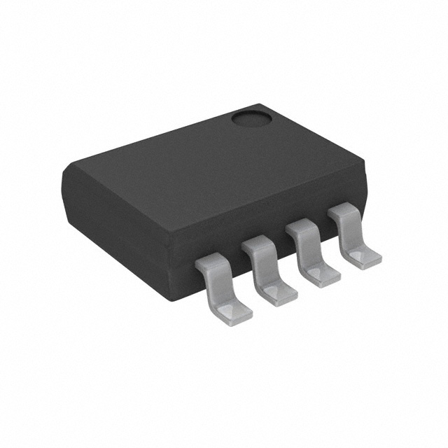
• 8-lead SOIC (0.150” Narrow and 0.208” Wide)
• 8-pad Ultra-Thin DFN (5 x 6 x 0.6 mm)
• 8-ball WLCSP (3 x 2 x 3 grid array)
• Die Wafer Form


