• Industry Standard Serial Interface
– IS25LP128F: 128Mbit/16Mbyte
– IS25WP128F: 128Mbit/16Mbyte
– 3 or 4 Byte Addressing Mode
– Supports Standard SPI, Fast, Dual, Dual
I/O, Quad, Quad I/O, SPI DTR, Dual I/O
DTR, Quad I/O DTR, and QPI
– Software & Hardware Reset
– Supports Serial Flash Discoverable
Parameters (SFDP)
• High Performance Serial Flash (SPI)
– 80MHz Normal Read
– Up to166Mhz Fast Read
– Up to 80MHz DTR (Dual Transfer Rate)
– Equivalent Throughput of 664 Mb/s
– Selectable Dummy Cycles
– Configurable Drive Strength
– Supports SPI Modes 0 and 3
– More than 100,000 Erase/Program Cycles
– More than 20-year Data Retention
• Flexible & Efficient Memory Architecture
– Chip Erase with Uniform Sector/Block
Erase (4/32/64 Kbyte)
– Program 1 to 256 Byte per Page
– Program/Erase Suspend & Resume
• Efficient Read and Program modes
– Low Instruction Overhead Operations
– Continuous Read 8/16/32/64 Byte
Burst Wrap
– Selectable Burst Length
– QPI for Reduced Instruction Overhead
– AutoBoot Operation
• Low Power with Wide Temp. Ranges
– Single Voltage Supply
IS25LP: 2.30V to 3.60V
IS25WP: 1.65V to 1.95V
– 10 mA Active Read Current
– 8 µA Standby Current
– 1 µA Deep Power Down
– Temp Grades:
Extended: -40°C to +105°C
Auto Grade (A3) : -40°C to +125°C
• Advanced Security Protection
– Software and Hardware Write Protection
– Advanced Sector/Block Protection
– Top/Bottom Block Protection
– Power Supply Lock Protection
– 4×256 Byte Dedicated Security Area
with OTP User-lockable Bits
– 128 bit Unique ID for Each Device
(Call Factory)
• Industry Standard Pin-out & Packages
– M =16-pin SOIC 300mil
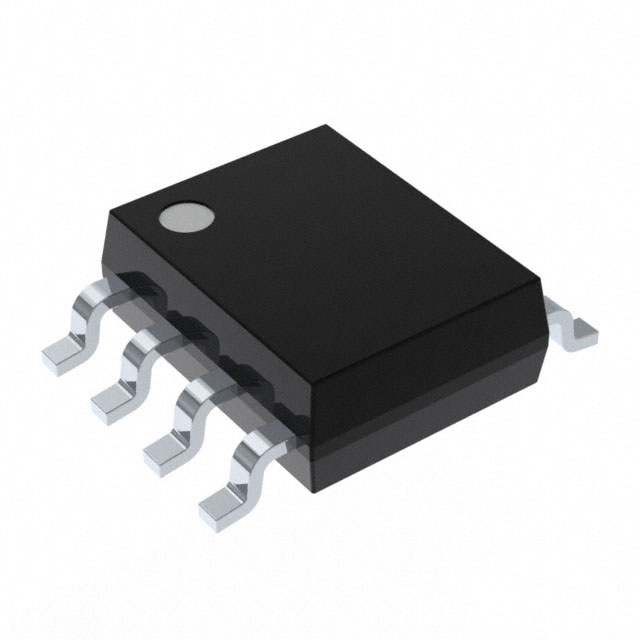
– B = 8-pin SOIC 208mil
– K = 8-contact WSON 6x5mm
– L = 8-contact WSON 8x6mm
– G = 24-ball TFBGA (4×6 ball array)
– H = 24-ball TFBGA (5×5 ball array)
– KGD (Call Factory)


