Single chip USB to asynchronous serial data
transfer interface.
Entire USB protocol handled on the chip. No
USB specific firmware programming required.
Fully integrated 1024 bit EEPROM storing
device descriptors and CBUS I/O configuration.
Fully integrated USB termination resistors.
Fully integrated clock generation with no
external crystal required plus optional clock
output selection enabling a glue-less interface
to external MCU or FPGA.
Data transfer rates from 300 baud to 3 Mbaud
(RS422, RS485, RS232) at TTL levels.
128 byte receive buffer and 256 byte transmit
buffer utilising buffer smoothing technology to
allow for high data throughput.
FTDI’s royalty-free Virtual Com Port (VCP) and
Direct (D2XX) drivers eliminate the
requirement for USB driver development in
most cases.
Unique USB FTDIChip-ID™ feature.
Configurable CBUS I/O pins.
Transmit and receive LED drive signals.
UART interface support for 7 or 8 data bits, 1
or 2 stop bits and odd / even / mark / space /
no parity
FIFO receives and transmits buffers for high
data throughput.
Synchronous and asynchronous bit bang
interface options with RD# and WR# strobes.
Device supplied pre-programmed with unique
USB serial number.
Supports bus powered, self-powered and highpower bus powered USB configurations.
Integrated +3.3V level converter for USB I/O.
Integrated level converter on UART and CBUS
for interfacing to between +1.8V and +5V
logic.
True 5V/3.3V/2.8V/1.8V CMOS drive output
and TTL input.
Configurable I/O pin output drive strength.
Integrated power-on-reset circuit.
Fully integrated AVCC supply filtering – no
external filtering required.
UART signal inversion option.
+3.3V (using external oscillator) to +5.25V
(internal oscillator) Single Supply Operation.
Low operating and USB suspend current.
Low USB bandwidth consumption.
UHCI/OHCI/EHCI host controller compatible.
USB 2.0 Full Speed compatible.
-40°C to 85°C extended operating temperature
range.
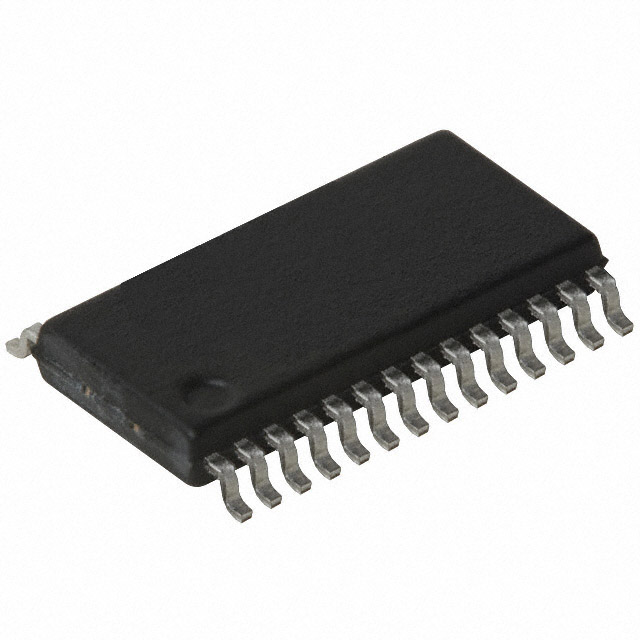
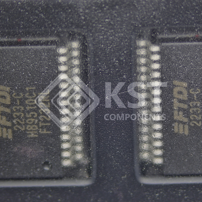
Available in compact Pb-free 28 Pin SSOP and
QFN-32 packages (both RoHS compliant).


