SN74LVC2G34DCKR

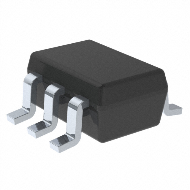
The SN74LVC2G34 device is a dual buffer gate designed for 1.65-V to 5.5-V VCC operation. The SN74LVC2G34 device performs the Boolean function Y = A in positive logic.

NanoFree package technology is a major breakthrough in IC packaging concepts, using the die as the package.

This device is fully specified for partial-power-down applications using Ioff. The Ioff circuitry disables the outputs, preventing damaging current backflow through the device when it is powered down.

Category:

Download Details PDF

Notice:

In stock will ship in 2 days. Real-time inventory pls confirm with us.

INQUIRY ONLINE


    SPECIFICATION

    • Available in the Texas Instruments NanoFree Package
    • Supports 5.5-V VCC Operation
    • Inputs Accept Voltages to 5.5 V
    • Maximum tpd of 4.1 ns at 3.3 V
    • Low Power Consumption, 10-µA Maximum ICC
    • ±24-mA Output Drive at 3.3 V
    • Typical VOLP (Output Ground Bounce) <0.8 V at VCC = 3.3 V, TA = 25°C
    • Typical VOHV (Output VOH Undershoot) >2 V at VCC = 3.3 V, TA = 25°C
    • Ioff Supports Live Insertion, Partial-Power-Down Mode, and Back-Drive Protection
    • Can Be Used as a Down Translator to Translate Inputs From a Maximum of 5.5 V Down to the VCC Level
    • Latch-Up Performance Exceeds 100 mA Per JESD 78, Class II
    • ESD Protection Exceeds JESD 22
      • 2000-V Human Body Model (A114-A)
      • 200-V Machine Model (A115-A)
      • 1000-V Charged-Device Model (C101)